- 您现在的位置:买卖IC网 > Sheet目录318 > CAV24C16YE-GT3 (ON Semiconductor)IC EEPROM I2C SRL 16KB 8TSSOP
�� �
�
�CAV24C02,� CAV24C04,� CAV24C08,� CAV24C16�
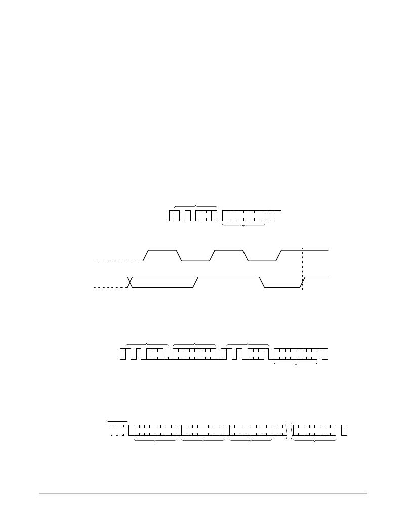
�READ� OPERATIONS�
�Immediate� Read�
�Upon� receiving� a� Slave� address� with� the� R/W� bit� set� to� ‘1’,�
�the� CAV24Cxx� will� interpret� this� as� a� request� for� data�
�residing� at� the� current� byte� address� in� memory.� The�
�CAV24Cxx� will� acknowledge� the� Slave� address,� will�
�immediately� shift� out� the� data� residing� at� the� current� address,�
�and� will� then� wait� for� the� Master� to� respond.� If� the� Master�
�does� not� acknowledge� the� data� (NoACK)� and� then� follows�
�up� with� a� STOP� condition� (Figure� 10),� the� CAV24Cxx�
�returns� to� Standby� mode.�
�Selective� Read�
�Selective� Read� operations� allow� the� Master� device� to�
�select� at� random� any� memory� location� for� a� read� operation.�
�The� Master� device� first� performs� a� ‘dummy’� write� operation�
�by� sending� the� START� condition,� slave� address� and� byte�
�address� of� the� location� it� wishes� to� read.� After� the�
�CAV24Cxx� acknowledges� the� byte� address,� the� Master�
�device� resends� the� START� condition� and� the� slave� address,�
�this� time� with� the� R/W� bit� set� to� one.� The� CAV24Cxx� then�
�responds� with� its� acknowledge� and� sends� the� requested� data�
�byte.� The� Master� device� does� not� acknowledge� the� data�
�(NoACK)� but� will� generate� a� STOP� condition� (Figure� 11).�
�Sequential� Read�
�If� during� a� Read� session,� the� Master� acknowledges� the� 1� st�
�data� byte,� then� the� CAV24Cxx� will� continue� transmitting�
�data� residing� at� subsequent� locations� until� the� Master�
�responds� with� a� NoACK,� followed� by� a� STOP� (Figure� 12).�
�In� contrast� to� Page� Write,� during� Sequential� Read� the�
�address� count� will� automatically� increment� to� and� then�
�wrap� ?� around� at� end� of� memory� (rather� than� end� of� page).�
�SCL�
�BUS� ACTIVITY:�
�MASTER�
�SLAVE�
�8�
�S�
�T�
�A�
�R�
�T�
�S�
�SLAVE�
�ADDRESS�
�A�
�C�
�K�
�9�
�D� ATA�
�BYTE�
�N�
�O�
�S�
�A� T�
�C� O�
�K� P�
�P�
�SDA�
�8� th� Bit�
�DATA� OUT�
�NO� ACK�
�STOP�
�Figure� 10.� Immediate� Read� Sequence� and� Timing�
�BUS� ACTIVITY:�
�MASTER�
�S�
�T�
�A�
�R�
�T�
�SLAVE�
�ADDRESS�
�ADDRESS�
�BYTE�
�S�
�T�
�A�
�R�
�T�
�SLAVE�
�ADDRESS�
�N�
�O�
�S�
�A� T�
�C� O�
�K� P�
�S�
�S�
�P�
�SLAVE�
�A�
�C�
�K�
�A�
�C�
�K�
�A�
�C�
�K�
�D� ATA�
�BYTE�
�Figure� 11.� Selective� Read� Sequence�
�BUS� ACTIVITY:�
�MASTER�
�SLAVE�
�ADDRESS�
�A�
�C�
�K�
�A�
�C�
�K�
�A�
�C�
�K�
�N�
�O�
�S�
�A� T�
�C� O�
�K� P�
�P�
�SLAVE�
�A�
�C�
�K�
�D� ATA�
�BYTE�
�n�
�D� ATA�
�BYTE�
�n+1�
�D� ATA�
�BYTE�
�n+2�
�D� ATA�
�BYTE�
�n+x�
�Figure� 12.� Sequential� Read� Sequence�
�http://onsemi.com�
�8�
�发布紧急采购,3分钟左右您将得到回复。
相关PDF资料
CAV24C32YE-GT3
IC EEPROM I2C SRL 32KB 8TSSOP
CAV24C64YE-GT3
IC EEPROM I2C SRL 64KB 8TSSOP
CAV4201TD-GT3
IC LED DVR 350MA STP-DN TSOT23-5
CB-1377
PANEL ALUMINUM CHASSIS
CBC5300-24C
ENERCHIP EH CBC5300 MODULE
CC-ACC-MX51-ETM
ADAPTER TRACE ETM/ETB JTAG
CDBMCU-DEBUG
EVAL BD FOR DSP CS48X & CS49X
CEL2MUSB
E2GO CELL PHONE CHARGER USB
相关代理商/技术参数
CAV24C256WE-GT3
制造商:ON Semiconductor 功能描述:256KB I2C SER EEPROM - Tape and Reel 制造商:ON Semiconductor 功能描述:REEL / 256KB I2C SER EEPROM
CAV24C256YE-GT3
制造商:ON Semiconductor 功能描述:256KB I2C SER EEPROM - Tape and Reel
CAV24C32C4CTR
功能描述:IC EEPROM 32KB I2C SER 4WLCSP 制造商:on semiconductor 系列:汽车级,AEC-Q100 零件状态:在售 存储器类型:非易失 存储器格式:EEPROM 技术:EEPROM 存储容量:32Kb (4K x 8) 时钟频率:400kHz 写周期时间 - 字,页:5ms 访问时间:900ns 存储器接口:I2C 电压 - 电源:2.5 V ~ 5.5 V 工作温度:-40°C ~ 125°C(TA) 标准包装:5,000
CAV24C32WE-GT3
功能描述:电可擦除可编程只读存储器 32KB I2C SER 电可擦除可编程只读存储器
RoHS:否 制造商:Atmel 存储容量:2 Kbit 组织:256 B x 8 数据保留:100 yr 最大时钟频率:1000 KHz 最大工作电流:6 uA 工作电源电压:1.7 V to 5.5 V 最大工作温度:+ 85 C 安装风格:SMD/SMT 封装 / 箱体:SOIC-8
CAV24C32YE-GT3
功能描述:电可擦除可编程只读存储器 32KB I2C SER 电可擦除可编程只读存储器 RoHS:否 制造商:Atmel 存储容量:2 Kbit 组织:256 B x 8 数据保留:100 yr 最大时钟频率:1000 KHz 最大工作电流:6 uA 工作电源电压:1.7 V to 5.5 V 最大工作温度:+ 85 C 安装风格:SMD/SMT 封装 / 箱体:SOIC-8
CAV24C512HU5EGT3
功能描述:IC EEPROM 512KBIT I2C 制造商:on semiconductor 系列:汽车级,AEC-Q100 零件状态:在售 存储器类型:非易失 存储器格式:EEPROM 技术:EEPROM 存储容量:512Kb (64K x 8) 时钟频率:1MHz 写周期时间 - 字,页:5ms 访问时间:400ns 存储器接口:I2C 电压 - 电源:2.5 V ~ 5.5 V 工作温度:-40°C ~ 125°C(TA) 标准包装:3,000
CAV24C512WE-GT3
功能描述:电可擦除可编程只读存储器 512KB I2C SER 电可擦除可编程只读存储器 RoHS:否 制造商:Atmel 存储容量:2 Kbit 组织:256 B x 8 数据保留:100 yr 最大时钟频率:1000 KHz 最大工作电流:6 uA 工作电源电压:1.7 V to 5.5 V 最大工作温度:+ 85 C 安装风格:SMD/SMT 封装 / 箱体:SOIC-8
CAV24C512YE-GT3
功能描述:电可擦除可编程只读存储器 512KB I2C SER 电可擦除可编程只读存储器 RoHS:否 制造商:Atmel 存储容量:2 Kbit 组织:256 B x 8 数据保留:100 yr 最大时钟频率:1000 KHz 最大工作电流:6 uA 工作电源电压:1.7 V to 5.5 V 最大工作温度:+ 85 C 安装风格:SMD/SMT 封装 / 箱体:SOIC-8